industrial switching power supply, switching power supply, industrial power supply
TOP250Y industrial switching power supply design
I know I think the best products of PI products are TOP250Y, TOP250Y only three or four peripheral components, which makes the power of the same design size smaller, standby efficiency higher and lower system cost, and maintain a wide range of uses and the style of the design is simple, make the design for the application under 290 w power supply to create cost-effective solutions.
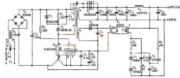
The switching power supply circuit composed of TOP250Y has an ac input voltage range of 176 ~ 264V, and the power supply efficiency can reach 86% at full load. The ac voltage UI obtains the dc high voltage successively through the electromagnetic interference (EMI) filter (C1, L1) and the input rectifier filter (V1, C2). The dc high voltage is connected to the L end of N1 after R1, providing voltage feedforward signal for TOP250Y, realizing overvoltage protection, undervoltage protection and Dmax function of changing the power supply with the input voltage. Here, the X pin of N1 is grounded to make TOP250Y work in the maximum duty ratio. Therefore, the maximum continuous output power (PoM) can be achieved even in a wide range of inputs (PoM=290W). Ground the F pin of N1 to make TOP250Y work at a higher frequency of 132kHz. This design method allows the high-frequency transformer to choose a smaller magnetic core and prevents magnetic saturation. After the secondary voltage passes through the rectifier filter of V5, C8 ~ C11, L2 and C12, the stable voltage output of + 24V/12A is obtained. C8 ~ C11 filter ripple voltage, L2 and C12 are used to eliminate switching noise. The power supply adopts a simple series voltage stabilizing tube type optocoupler feedback circuit. E1 is 4N25 type linear optical coupler. The V7 and V8 adopt 1N963 and 1N962 regulator tubes respectively. The voltage stabilizing principle is as follows: when the output voltage increases Uo due to some reason, the resulting error voltage makes the IF of LED in E1 become larger, and the IE of the optocoupler receiver increases, making the current Ic at the N1 control end become larger, while the duty cycle D decreases, resulting in the decrease of Uo, thus achieving the voltage stabilizing purpose. On the contrary, Uo↓→I F↓→I E↓→Ic↓→D↑→Uo↑, also plays a stabilizing role. When switching power supply is empty, TOP250Y can greatly reduce the maximum output duty ratio by skipping cycles, making Dmax<2%. Therefore, there is no need to connect false load at the output end, which can also reduce the power consumption in no-load or standby state. V6 and C14 provide soft start for the secondary, and C14 is the soft start capacitor, which can eliminate the voltage overshoot phenomenon when the power supply is just connected, so that the C pin voltage provided by the feedback winding to N1 is prior to the output voltage. This ensures that the output voltage can be properly adjusted at startup even at low input voltage and full load. Resistance R5 and capacitance C13 constitute control loop compensation circuit. After the feedback winding voltage goes through the V4 and C5 rectifier filtering, the feedback voltage of 12v is generated, and the bias voltage is provided to the TOP250Y control end through E1. The C4 is a by-pass capacitor, which also forms a compensation circuit for the control loop with R3 and C3. The zener clamp tube V2, ultra - fast diode V3, resistor R2 and capacitor C6 constitute the peak absorption circuit. It is used to absorb the peak voltage generated by the leakage inductance of the high-frequency transformer when TOP250Y is cut off, and it can protect the drain pole of the MOSFET tube in TOP250Y. Since R2 and C6 are connected in parallel on V2, R2 is responsible for almost all the discharge energy in normal operation, and in the case of startup or overload, V2 limits the peak voltage to no more than the safety voltage (700V) of N1 MOSFET tube.

 Request A Quote