Switch power supply design
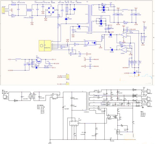
The three-way isolated output +15V, +15V and +5V switching power supply circuit constituted by TOP247YN is shown in the figure. Its input voltage range is 20-30v DC and 85-265v AC.
The model of the rectifier bridge is RS205, the parameter is reverse voltage 600V, and the maximum passable current is 2A.
The primary protection circuit is composed of clamping circuit (D5, D8), which can effectively suppress the peak voltage caused by leakage inductance of high-frequency transformers and protect the power switch tube inside TOP247YN from damage. D8 adopts P6KE200A type transient voltage suppression diode (TVS), and its reverse breakdown voltage UB=200V. V5 uses UF4007 ultra - fast recovery diode (SRD).
C5 is the bypass capacitor of VCC terminal.
D6 and C13 constitute a high frequency rectifier filter at the output end of the feedback coil.
The secondary high-frequency rectifier tube is a schottky diode with high current and low voltage drop, model 21DQ10 (3A/100V). It also USES UF4007. There is a filter circuit behind, and the output terminal is connected with a false load.
The ferrite core model is EE25. In order to prevent the occurrence of magnetic saturation phenomenon, it is necessary to add a certain air gap.
2. Areas for improvement
The above is a direct mapping of the transmitter switching power supply part of the circuit diagram. After analysis, there is still room for improvement, mainly in the following two aspects.
1). It can also be in the transformer primary and RC absorption circuit, namely on the D8 Ω parallel R = 68 k / 2 w, C = 4.7 nF / 1000 v.
2). For the output filter part, the filter capacitance value is small and there is no inductance connection, which will lead to large fluctuation of output voltage, and there is a fuse connected to the output end, I don't know why.
3. The analysis and calculation of the core part
In addition, there are two aspects to pay attention to, the need for more detailed analysis and calculation, in order to have a deeper understanding of the working principle of the circuit.
1). TOP247YN external pin connection.TOP247YN belongs to the fourth generation of TOP Switch-GX series single chip Power supply chip launched by PI (Power Integration) company. The chip has six pins in total. In addition to the required C (control), D (drain) and S (source), it also has three characteristic pins L (line voltage detection), X (external current limiting) and F (frequency). Line voltage detecting pin can realize overvoltage (OV), under voltage (UV) and other functions. External limiting pin can realize external limiting regulation and remote on/off control. The frequency pin can control the switching frequency of 66kHz or 132kHz.
In this circuit, all functions of the line voltage detection pin are disabled when it is connected to the source pin. When the frequency pin is connected to the source, the switching frequency is 132kHz. External current limiting resistance R = 27 k pin receive Ω, corresponding current-limiting Ilimit = 40% * 3.60 = 1.44 A.
2). The design of high-frequency transformers, that is, the size of transformers and parameters of enameled wires, such as wire diameter and number of turns, are closely related to these parameters and power output capacity, namely the output current of each circuit.
|
Input Min |
85vac |
Input Max |
265vac |
|
Output 1 |
5VDC |
Io |
0.5A |
|
Output 2 |
15VDC |
Io |
0.1A |
|
Output 3 |
15VDC |
Io |
0.1A |
|
NVcc |
12VDC |
Io |
0.01A |
|
Dmax |
0.48 |
|
|
|
Operating Frequency Fs |
132kHz |
|
|
|
Input capacitance |
10uF |
IN ripple voltage |
27.94V |
Step 1: o CORE (CORE) AP = AW * Ae = (* 10000) for Pt/fs (2 Δ B * * J * Ku) transmit power Pt = + Po Po/eta
J: current density of A/cm2 (300 ~ 500) generally from 350 to 400, Ku: winding coefficient is 0.2 ~ 0.5 generally take 0.4, η = 0.75 ~ 0.85, generally take 0.8, △ B = 0.185 T usually take 0.2 or below.
Pt = Po /η +Po = 12.375W AP = AW*Ae = (12.375*10000)/(2*0.185*132*350*0.4) = 0.00335 (cm²)
Step 2: estimation of critical current IOB(DCM/CCM BOUNDARY, critical mode is between 60~80%, take 0.75)
0.75 * 0.5 = 0.375 A
Step 3: find the ratio of turns N = [VIN(min)/(Vo + Vf)] * [Dmax/(1-dmax)]
Dc input is taken here, and the ripple is included into Vo, main output voltage, Vf, diode voltage drop, and 0.7v is taken.
VIN(min)= 85.16 V
Turn ratio: N = [85.16 / (5 + 0.7)] * [0.48 / (1-0.48)] = 13.79
Step 4: asks the CCM/DCM critical state deputy side peak current Δ ISB
ΔIsb = 2Iob / (1-Dmax) = 1.44 A
Step 5: calculate secondary inductance Ls and primary inductance Lp
Ls =(Vo + Vf)(1-Dmax) * Ts / Δisb = (5 + 0.7)(1 – 0.48) * 7.6*10e-6 /1.44 = 15.6 uH
Here, Vf is the diode voltage drop of 0.7v, Ts is the switching cycle 1/Fs.
Lp = n ^ 2 * Ls revised = 2974 uh - > 3 mH
Step 6: for CCM when vice side peak current Δ Isp. The CCM in the original edge peak current Δ Ipp
ΔIsp = Io(max)/(1-Dmax)+(ΔISB/2) = 0.5 / 0.52 + 1.44 / 2 = 1.68A
ΔIpp= ΔIsp/N = 0.12 A
Step 7: calculate the diameter of each winding wire number wire diameter
Check wire diameter specification table here. Divide the maximum average current flow by the set current density. In order to eliminate the skin effect, the line diameter should not exceed 0.5, depending on the frequency of the switch, you can check the relevant information here.
R = 0.5/350 R = 0.21mm skin effect copper wire penetration depth △=66.1 / [SQRT (fs)] = 0.18mm
You can see that you can't use a single enameled wire. There are two options. One is to use multiple wire, and the other is to use multiple wire. Multiple strands are selected and wound.
Calculate the primary Np line diameter =1 * 0.18 (root number * diameter)
Calculate secondary Ns1 linediameter =4 * 0.1
Calculate secondary Ns2 linediameter =1 * 0.18
Step 8: determine Np, Ns , every turn volts (Va = (Vo + Vf)/Ns)
1) Np = Lp * Δ Ipp/Ae (Δ B *) = 104
2) Ns = Np/n =7.54 corrected 8T
3) Ns2= (Vo2+Vf) /Va=20.77 corrected 21T
4) Nvcc = (Vcc + Vf)/Va = 16.79 corrected 17T
The number of turns is only an approximate value, which should be slightly adjusted in the actual test to achieve the best.
After that, I'll write about other switching power supply. We are
MICRO POWER ELECTRONICS (HK) CO., LIMITED, mainly engaged in smps design, power supply designs, switch mode power supply, smps switching power supply design, high power switching power supply design, power switch design, switching power supply, switch mode power supply, switching power supply design, ac dc switching power supply. If you are interested in, you can visit our official website at
micropowerchina.com.

 Request A Quote