switch power supply design experience
Switch Power Supply Design Experience
Firstly, start from switching power supply design and production process description, about PCB design. Switching power supply is a special kind of analog circuit which works at high frequency and high pulse. Board layout shall follow the principle of high frequency circuit wiring.
Layout: the connection line of pulse voltage shall be as short as possible, including the connection line from the input switch tube to the transformer and the connection line from the output transformer to the rectifier tube. The pulse current loop should be as small as possible, such as input filter capacitance positive to transformer and return capacitance negative to switching tube. The output portion of the transformer from the outlet to the rectifier tube to the output is as close as possible to the switching power supply input when the output capacitance returns to the X capacitance in the transformer circuit. The input line should not be parallel to other circuits and should be avoided. The Y capacitor shall be placed at the housing ground terminal or FG connection terminal. The common touch inductance keeps a certain distance from the transformer to avoid magnetic coupling. If it is difficult to deal with, a shield can be added between the common inductor and the transformer. The above items have a great impact on the EMC performance of the switching power source.
Generally, two capacitors with one close to the rectifier tube and the other close to the output terminal can affect the output ripple index of the power supply. The parallel effect of two small-capacity capacitors should be better than that of one large-capacity capacitor. The heating element should keep a certain distance from the electrolytic capacitor. The heating element should be kept at a certain distance from the electrolytic capacitor to extend the life of the whole machine. The electrolytic capacitor is the bottleneck of the life of the switching power supply. For example, the transformer, power tube and high-power resistor should be kept at a distance from the electrolysis, and the space for heat dissipation must be left between the electrolysis. If conditions permit, it can be placed in the air inlet.
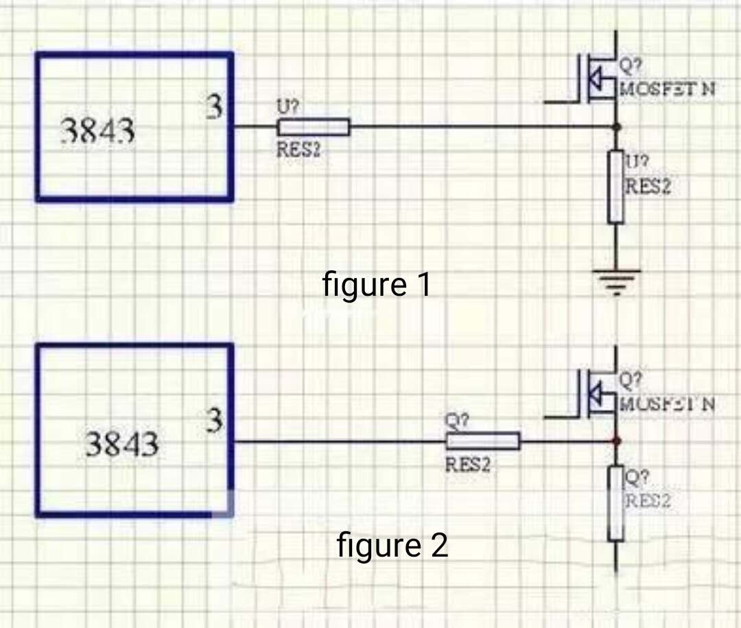
Attention should be paid to the control part: the connection line of the weak signal circuit with high impedance should be as short as possible, such as the sampling feedback loop, and the interference and current sampling signal circuit should be avoided as far as possible during the processing, especially the current control circuit. Some of these techniques are illustrated by the 3843 circuit as shown in figure (1). The effect of figure 1 is better than that of figure 2, in which the current waveform observed by oscilloscope at full load is obviously superimposed with spikes. As the interference current limiting point is lower than the design value, there is no such phenomenon in figure 1. There are also switch tube drive signal circuit, switch tube drive resistance to be close to the switch tube, can improve the reliability of the switch tube, this power MOSFET high dc impedance voltage drive characteristics.
Here are some principles of PCB wiring.
Line spacing: with the continuous improvement of PCB technology, the line spacing of general processing plants is equal to or even less than 0.1mm. There is no problem, fully able to meet most applications. Considering the components and production process used in the switching power supply, the minimum line spacing of the double panel is generally set as 0.3mm, the minimum line spacing of the single panel is set as 0.5mm, and the minimum spacing of the welding plate and the welding plate, the welding plate and the through hole or the through hole and the through hole is set as 0.5mm, so as to avoid the phenomenon of "Bridging" in the welding operation process. In this way, most board manufacturers can easily meet the production requirements, and can control the yield very high, but also achieve a reasonable wiring density and a more economical cost.
The minimum line spacing is only suitable for the signal control circuit and low-voltage circuit with voltage lower than 63V. When the line voltage is greater than this value, the line spacing can be generally taken according to the empirical value of 500V/1mm.
In view of some relevant standards that have clear provisions on line spacing, they should be strictly implemented in accordance with the standards, such as connecting the ac inlet end to the fuse end. Some power supplies have high volume requirements, such as modular power supplies. In general, the transformer input side line spacing of 1mm has been proved to be feasible. For ac input and (isolated) dc output power supply products, it is strictly stipulated that the safe spacing should be greater than or equal to 6mm. Of course, this is determined by the relevant standards and implementation methods. In general, the safe distance can be taken as a reference by the distance on both sides of the feedback optical coupler, and the principle is greater than or equal to this distance. It can also be grooved on the printed board under the photocoupler to increase the creepage distance to meet the insulation requirements. In general, the wiring on the ac input side of the switching power supply or the distance between the components on the board and the non-insulated shell and radiator shall be more than 5mm, and the distance between the wiring on the output side or the components and the shell or radiator shall be more than 2mm, or strictly in accordance with the safety regulations.
Common methods: the circuit board slotting method mentioned above is suitable for some occasions with insufficient spacing. This method, by the way, is also commonly used as a protective discharge gap, commonly found in the television picture tube tail plate and the power supply ac input. The method has been widely used in the module power supply, and good results can be obtained under the condition of encapsulation.
Method two: pad insulation paper, can use green shell paper, polyester film, ptfe directional film insulation materials. General power supply with green paper or polyester film pad in the circuit board in the metal housing, the material has high mechanical strength, there is a certain ability to resist moisture. Ptfe directional film has been widely used in module power supply due to its high temperature resistance. An insulating film can also be placed between the element and the surrounding conductor to improve the electrical resistance of the insulation.
Note: some devices insulation coating should be used as insulating medium decreased clearance, such as the outside of electrolytic capacitors, under the condition of high temperature, the skin may heat shrink. The front end of the large electrolytic explosion-proof groove should be left with space to ensure that the electrolytic capacitor can unimpeded discharge pressure under extraordinary circumstances.
About the PCB copper wiring:
Wiring current density: nowadays most electronic circuits are made of copper tied with insulating board. Common circuit board copper thickness of 35 m, wiring can be based on 1A/mm experience value of the current density value, the specific calculation can be referred to the textbook. In order to ensure the mechanical strength of wiring, the line width should be greater than or equal to 0.3mm(other non-power circuit boards may have a smaller minimum line width). Copper 70 m circuit boards are also commonly used in switching power supplies where current density may be higher.
Add a point, now commonly used circuit board design tools software generally have design specifications, such as line width, line spacing, dry disk through hole size parameters can be set. When designing the circuit board, the design software can be automatically executed according to the specifications, which can save a lot of time, reduce part of the workload and reduce the error rate.
Generally, double panels can be used for lines with high reliability requirements or high wiring density. Its characteristics are moderate cost, high reliability, can meet most applications.
Part of the module power supply line also adopts multi-layer board, which is mainly convenient for integrating transformer inductor and other power devices, optimizing wiring and cooling power pipe. It has the advantages of good process appearance and consistency and good heat dissipation of transformers, but its disadvantages are high cost and poor flexibility, which is only suitable for large-scale industrial production.
Single panel, market circulation general switch power supply almost all use a single sided circuit board, which has the advantage of low cost, in the design, and the production process to take some measures to ensure its performance.
Some experiences about the design of single sided PCB are discussed. Because the single panel has the characteristics of low cost and easy to make, it has been widely used in switching power lines. Since it has only one side of copper, the electrical connection and mechanical fixation of the device all depend on that layer of copper, which must be handled with care.
In order to ensure good welding mechanical structure performance, the single panel welding plate should be slightly larger, to ensure that the copper sheet and the substrate good bonding force, and not be subjected to shock when the copper sheet stripping, breaking. General welding ring width should be greater than 0.3mm. The diameter of the hole should be slightly larger than the diameter of the device pin, but should not be too large, to ensure the shortest solder connection distance between the pin and the pad. The size of the disc hole shall not interfere with the normal inspection. The diameter of the welding disc hole is generally larger than the diameter of the pin 0.1-0.2mm. Multi-pin devices can also be larger to ensure smooth inspection.
Electrical wiring should be as wide as possible, the principle width should be greater than the diameter of the pad.
Principle minimum line width should be greater than 0.5mm.
Single panel components should be attached to the circuit board. For devices requiring overhead heat dissipation, a bushing should be added to the pin between the device and the circuit board to support the device and increase insulation. To minimize or avoid the impact of external force impact on the connection between the disc and the pin, strengthen the strength of the welding. Heavy components on the circuit board can increase the support connection point, can strengthen the connection strength with the circuit board, such as transformer, power device radiator.
We are MICRO POWER ELECTRONICS (HK) CO., LIMITED. We are power supply supplier and switch power supplier, mainly engaged in Power Supply customization, including ac dc switching power supply, 24v power supply, smps switch mode power supply, 12v switch power supply, switching power supply design, 48v dc power supply, 24v switching power supply, smps power supply and High Power :1200w - 500kW. AC and DC Power Supply. If you are interested in, you can visit our official website at micropowerchina.com.

 Request A Quote